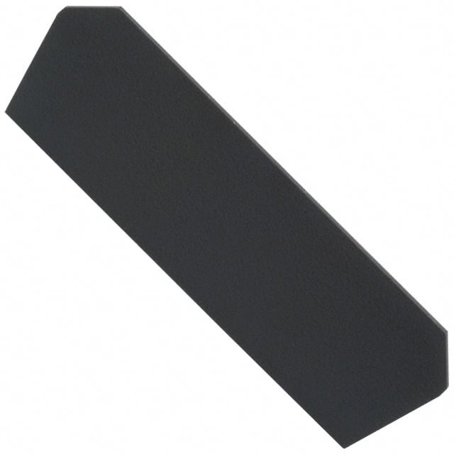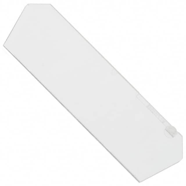
2003 Microsemi Corporation TRANS HBT RF BIPOLAR 55BT
Diskreetsed pooljuhid
Tootja number:
2003
Tootja:
Tootekategooria:
Kirjeldus:
TRANS HBT RF BIPOLAR 55BT
RoHs olek:
Andmetabelid:
Alalisvoolu võimendus (hFE) (min) @ Ic, Vce :
10 @ 100mA, 5V
Kasu :
8.5dB
Müra näitaja (dB tüüp @ f) :
-
Osa olek :
Obsolete
Paigaldustüüp :
Chassis Mount
Pakend/ümbris :
55BT-1
Pakendamine :
Bulk
Pinge – kollektori emitteri rike (maksimaalne) :
50V
Sagedus – üleminek :
2GHz
seeria :
-
Tarnija seadmepakett :
55BT-1
Töötemperatuur :
200°C (TJ)
Transistori tüüp :
NPN
Võimsus – max :
12W
Vool – koguja (Ic) (maksimaalne) :
500mA
Laos
45,439
Ühiku hind:
Võtke meiega ühendust Pakkumine
2003 Konkurentsivõimelised hinnad
ChipIcil on ainulaadne tarneallikas. Pakume oma klientidele 2003 konkurentsivõimelise hinnaga. Saate nautida meie parimat teenust, ostes ChipIc 2003. Parima hinna saamiseks saidil 2003 võtke meiega ühendust.
Hinnapakkumise saamiseks klõpsake
2003 Iseärasused
2003 is produced by Microsemi Corporation, belongs to Transistorid – bipolaarsed (BJT) – RF.
2003 Toote üksikasjad
:
2003 – Transistorid – bipolaarsed (BJT) – RF disainitud puhvervõimendid ja toodetud Microsemi Corporation.
2003, mida pakub Microsemi Corporation, saab osta CHIPMLCC-st.
Siit leiate erinevaid juhtivate tootjate elektroonilisi osi rahu.
CHIPMLCC 2003 on range kvaliteedikontrolliga ja nõuetele vastav kõike nõuetele.
CHIPMLCC-s näidatud fondi staatus on ainult viitamiseks.
Kui te ei leia otsitavat osa, võtke meiega ühendust lisateavet, näiteks varude arvu andmetabelis 2003 (PDF), hind 2003, Pinout 2003, manuaal 2003 Ja 2003 asenduslahendus.
2003 FAQ
:
1. Q: What is the difference between a diode and a transistor?
A: A diode is a two-terminal electronic component that allows current to flow in one direction only, while a transistor is a three-terminal device used for amplification and switching purposes.
2. Q: How does a semiconductor work as a conductor?
A: Semiconductors can conduct electricity under certain conditions due to their ability to change from insulating to conducting state when exposed to an electric field or light.
3. Q: What are the main challenges in fabricating high-quality silicon wafers?
A: The main challenges in fabricating high-quality silicon wafers include controlling impurities, achieving uniform crystal structure, and minimizing defects during the manufacturing process.
4. Q: Can you explain the concept of doping in semiconductors?
A: Doping involves intentionally introducing impurities into a semiconductor to alter its electrical properties, such as creating n-type or p-type regions to control conductivity.
5. Q: What are the key differences between CMOS and bipolar transistors?
A: CMOS transistors consume less power and have higher noise immunity compared to bipolar transistors, making them suitable for integrated circuits with low power requirements.
6. Q: How do photolithography techniques contribute to semiconductor manufacturing?
A: Photolithography is used to transfer patterns onto semiconductor wafers, allowing for precise etching and deposition processes to create intricate circuitry and components.
7. Q: What role does the cleanroom environment play in semiconductor fabrication?
A: Cleanrooms provide a controlled environment with low levels of airborne particles to prevent contamination during the delicate processes involved in semiconductor fabrication.
8. Q: Can you explain the concept of electron mobility in semiconductors?
A: Electron mobility refers to the speed at which electrons move through a semiconductor material under the influence of an electric field, impacting the material's overall conductivity.
9. Q: What are the primary methods for testing the quality and performance of semiconductor devices?
A: Semiconductor devices are typically tested using techniques such as electrical characterization, reliability testing, and failure analysis to ensure their functionality and durability.
10. Q: How do advancements in semiconductor technology impact the development of electronic devices?
A: Advancements in semiconductor technology enable the creation of smaller, more efficient, and higher-performing electronic devices, driving innovation across various industries.
2003 Seotud märksõnad
:
2003 Hind
2003 Maalimine
2003 Tihvtide pinge
Pakkumised: Kiire hinnapakkumise kontroll
Minimaalne tellimus: 1
Sisaldab "2003" seeria tooteid